top of page
Lab for Electron Tomography & Coherent Imaging
電子斷層��暨同調顯影實驗室
With the significant advances and applications of 2D materials, imaging, understanding, and further manipulating new 2D materials have become a prominent research topic in condensed matter sciences. A common example is graphene, a major material for optoelectronics and photodetection applications. Studies have predicted that grain boundaries play a major role in the electronic, chemical, and magnetic properties of 2D materials. Therefore, imaging the atomic arrangement of materials of interests, such as defects and grains, is a crucial topic for optoelectronics and photodetection applications.
To image 2D materials at atomic resolution, using beams of electrons (instead of other sources such as photons or neutrons) seems to be a more favorable alternative because of the considerably larger scattering cross-section and shorter wavelength of electrons. Recently, atomic resolution imaging of 2D materials has been achieved through various transmission electron microscopy (TEM) techniques such as bright-field TEM imaging and scanning transmission electron microscopy with an annular dark-field imaging. However, these techniques are conducted at relatively high electron energy levels. Moreover, radiation damage is a critical concern in 2D materials. A direct method of reducing radiation damage is the use of low-energy electron beams. However, once the energy level is reduced below 10 keV, the achieved spatial resolution also deteriorates to only a few nanometers, which is extremely low for revealing the atomic information of 2D materials. Another challenge in TEM techniques is lens selection. Acquiring high-quality TEM images depends on optimizing the combination of condensers and objective lenses. Aberration, coherence, and brightness considerably affect image quality and render the resulting image difficult to interpolate.
The aforementioned problems can be overcome using a single-atom-tip (SAT) electron source. The advantage of using an SAT source is that the electron energy can be reduced while maintaining coherence. The electrons emitted from the single atom at the end of the tip are apparent with high coherence as from a point source; hence, applying a concept similar to that of coherent diffraction imaging (CDI) (also called lensless imaging) seems to be a promising approach for obtaining 2D images at atomic resolution. Theoretically, considerably few high-energy electrons are scattered from low-Z elements; the low-Z elements would be almost invisible if only the scattered electrons are collected. Moreover, if the electron energy is reduced, the cross-section becomes larger. Hence, low-energy electrons provide an excellent opportunity to not only reduce radiation damage but also enhance the scattered signals of low-Z materials.
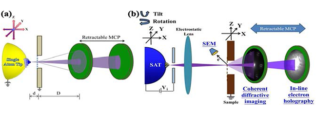
Schematic of SAT-CDI
(a) Lens-less transmission-type low-voltage coherent electron microscope
(b) Transmission-type low-kV coherent electron microscope

Comparison of experimental and reconstructed diffraction patterns.
(a) Experimental diffraction pattern.
(b) Central speckle of the experimental measurement. (c) Reconstructed diffraction pattern.
(d) Central speckle of the reconstructed pattern.
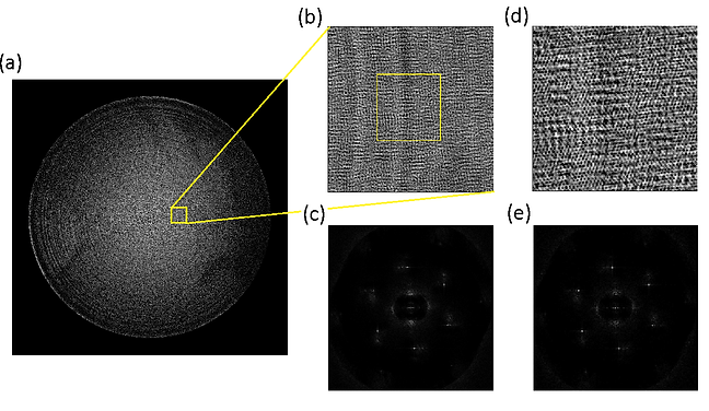
Real-space reconstruction from experimental diffraction pattern and zoomed views.
(a) Overview of the reconstructed image.
(b) Zoomed view of the yellow box shown in (a).
(c) Fourier transform of (b).
(d) Further zoomed view of the yellow box shown in (b).
(e) Fourier transform of (d). Sixfold honeycomb-like structures are clearly visible in panel (d).
bottom of page